| |
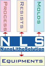
Nanolithosolution provides a comprehensive system for patterning 3D nanostructures with sub-20 nm resolution. Nanolithosolution's technology allows any facility to use its current photolithography equipment to achieve nano-scale patterning with precise and accurate overlay alignment. We provide all the necessary components and support, including:
Nano-fabrication module and controller,
Chemicals,
Auto ReleaseTM imprinting mold substrate,
and imprint fabrication process specifications.
Nanolithosolution’s technology is well-suited for customers in research and development, where traditional microscale photolithography resolution may not be sufficient.
Applications:
optical devices, displays, data storage, biotech, semiconductor ICs, chemical synthesis, and advanced materials.
|
 |